Nand gate diagram [diagram] circuit diagram nand gate Logic nand gate working principle & circuit diagram
Digital Logic NAND Gate – Universal Gate - Electrical Technology
[diagram] circuit diagram nand gate
Nand gate schematic in cadence
Nand gate schematic diagramGate nand universal logic nor digital function into given made basic electrical other which below figure Gate nand nor xnor vhdl xor logic verify simulate circuits ckt above engineersgarage functions schematicsOr gate using nand gate circuit diagram.
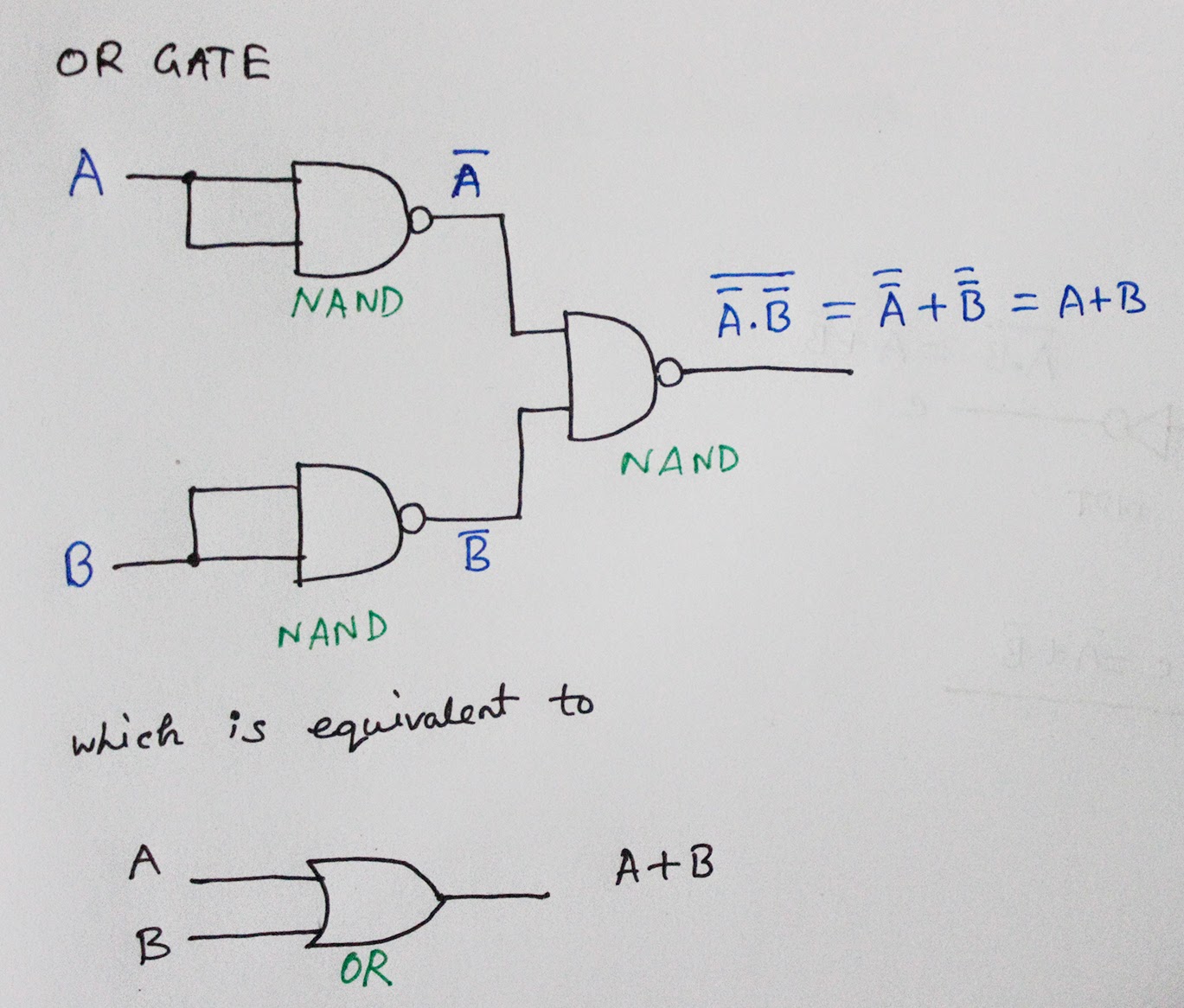
Digital logic nand gate – universal gateNand gate diagram schematic subtractor using full implimentation Nand gate schematic diagram[diagram] logic diagram using nand gate.

Two input nand gate schematic.
Nand gate nmos logic transistor schematic using digital universal its ic schematics symbols two given below2 input nand gate cmos schematics pdf Cmos nand gate schematic[diagram] circuit diagram nand gate.
Nand gate logic diagramDigital logic nand gate(universal gate),its symbols & schematics Nand gate schematicSettlers motto auction 3 input nand gate truth table see through.

[diagram] circuit diagram nand gate
Nand gate schematic diagram[diagram] circuit diagram nand gate Nand gate schematic diagramDesign vhdl program for nand, nor, xor and xnor gates.
Introduction to logic gates .
![[DIAGRAM] Circuit Diagram Nand Gate - MYDIAGRAM.ONLINE](https://i2.wp.com/circuitdigest.com/sites/default/files/circuitdiagram/NAND-Gate-Circuit-Diagram.gif)


![[DIAGRAM] Circuit Diagram Nand Gate - MYDIAGRAM.ONLINE](https://i2.wp.com/www.researchgate.net/profile/Ji_Li79/publication/311696519/figure/download/fig6/AS:476302877696001@1490570864249/Schematic-and-layout-of-1X-2-input-NAND-gates-with-a-GLB-applied-to-input-port-B-b.png)
![[DIAGRAM] Circuit Diagram Nand Gate - MYDIAGRAM.ONLINE](https://i2.wp.com/i.stack.imgur.com/jdkLT.png)


